Here we outline the steps to build a layered device, solve for the gate potentials, and visualize the results.
1) Import the components
import matplotlib.pyplot as plt
import numpy as np
from IPython.display import Image, display

from pescado.mesher import shapes
from tempura.electrostatics.device import Device, Dielectric, Gate, TwoDEG
from tempura.electrostatics.pescado_wrapper import build_problem, solve_gate_potentials
We start by importing geometry types, solver wrappers, and plotting utilities.
2) Define the XY grid and device size
size = 31
dx = 1.0
dy = 1.0
L = size * dx
W = size * dy
The script uses a square 31 x 31 grid with unit spacing.
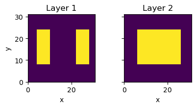
3) Build demo masks for gate layers
As an example geometyr, we use a two layer device created by make_demo_masks.
It creates the gate stencils used by the gate layers.
def make_demo_masks(nx, ny):
    """Create the two gate stencils used throughout the example."""
    mask_x = np.zeros((ny, nx), dtype=int)
    mask_y = np.zeros((ny, nx), dtype=int)

    # gate_layer_1: two independent finger gates.
    mask_x[8:24, 4:10] = 1
    mask_x[8:24, 22:28] = 1

    # gate_layer_2: one broad plunger gate.
    mask_y[8:24, 6:26] = 1

    return mask_x, mask_y


gate_layer_1, gate_layer_2 = make_demo_masks(size, size)
The masks are two-dimensional arrays of integers.
All non-zero values are treated as gates.
In this way, we can easily create arbitrary gate patterns by drawing them into the mask arrays.
We can visualize the masks with imshow to confirm they look as expected:
fig, ax = plt.subplots(ncols=2, figsize=(4.5, 2.2), sharex=True, sharey=True)
ax[0].imshow(gate_layer_1, origin="lower", extent=(0, L, 0, W), vmin=0)
ax[0].set_title("Layer 1")
ax[0].set_xlabel("x")
ax[0].set_ylabel("y")
ax[1].imshow(gate_layer_2, origin="lower", extent=(0, L, 0, W), vmin=0)
ax[1].set_title("Layer 2")
ax[1].set_xlabel("x")
plt.tight_layout()
5) Build the layered device stack
Layers are added in order from bottom to top.
Then finalize() computes the height maps and shape objects used by the solver pipeline.
We start by adding a substrate layer, then a TwoDEG layer, then two gate layers separated by dielectric blankets.
dev = Device(device_size=(L, W, dx, dy))
dev.add_layer(
    Dielectric(
        name="substrate",
        permitivity=12.9,
        resolution=np.array([dx, dy, 5.0]),
        thickness=10.1,
    )
)
dev.add_layer(
    TwoDEG(
        name="2deg",
        permitivity=12.9,
        resolution=np.array([dx, dy, 2.0]),
        thickness=2.1,
    )
)
dev.add_layer(
    Dielectric(
        name="blanket_0",
        permitivity=9.1,
        resolution=np.array([dx, dy, 2.0]),
        thickness=2.1,
    )
)
After the first three layers, we start adding the gate layers, which use the demo masks as stencils to define the gate shapes.
Each Gate requires a stencil to define the gate geometry, and the resolution parameter defines the grid spacing for meshing that layer.
Note
The resolution parameter is a 3D vector that defines the grid spacing in the x, y, and z directions for meshing that layer.
The x, y and z spacings should be sufficient to capture the details of the structure in each direction.
dev.add_layer(
    Gate(
        name="gate_layer_1",
        resolution=np.array([dx, dy, 2.0]),
        thickness=2.1,
        stencil=gate_layer_1,
    )
)
dev.add_layer(
    Dielectric(
        name="blanket_1",
        permitivity=9.1,
        resolution=np.array([dx, dy, 2.0]),
        thickness=2.1,
    )
)
dev.add_layer(
    Gate(
        name="gate_layer_2",
        resolution=np.array([dx, dy, 2.0]),
        thickness=2.1,
        stencil=gate_layer_2,
    )
)
Once the layers are added, we call finalize() to compute the height maps and shape objects used by the solver pipeline.
dev.finalize()
6) Build and solve the Poisson problem
build_problem creates the meshed electrostatic model, and
solve_gate_potentials factors the system once and solves the full gate basis
in one multi-right-hand-side pass.
pb, region_shapes, gate_names = build_problem(dev)
potentials, problem = solve_gate_potentials(pb, region_shapes, gate_names)
The returned potentials dictionary contains one solved vector per gate.
7) View the exported 3D device
Use the embedded viewer to inspect the stacked geometry directly.
If your browser blocks the embedded frame, open the viewer directly:
3D device viewer.
8) Compare the gate basis potentials
Each entry in potentials is a Green's function: the electrostatic solution when the corresponding gate is held at 1 V while all other gates are grounded.
The physical potential for any desired set of gate voltages is then a simple linear combination of these basis potentials.
We start by extracting the values at the 2DEG plane.
problem.points_inside returns the mesh-point indices that fall inside a given region shape, here region_shapes['2deg'].
Indexing into a basis-potential vector with those indices selects only the values at the 2DEG, which we then reshape back onto the square XY grid so it can be plotted with imshow.
indices = problem.points_inside(region_shapes['2deg'])
gate_layer_1 = potentials['gate_layer_1'][indices]
gate_layer_1 = gate_layer_1.reshape(size, size)

gate_layer_2 = potentials['gate_layer_2'][indices]
gate_layer_2 = gate_layer_2.reshape(size, size)

_potential = gate_layer_1 * 1 - gate_layer_2 * 2

fig, ax = plt.subplots(figsize=(5.5, 4.0), constrained_layout=True)
im = ax.imshow(
    _potential,
    vmin=-.25,
    vmax=.25,
    cmap="RdBu",
    origin="lower",
    extent=(0, L, 0, W),
)
fig.colorbar(im, ax=ax, label="Potential (V)", shrink=0.8)
<matplotlib.colorbar.Colorbar at 0x7f7fabedbb30>

Here _potential is a linear combination of the two basis potentials with gate voltages +1 V and −2 V respectively.
The red–blue colormap shows the signed potential at the 2DEG, making it easy to see which regions are electrostatically depleted or enhanced by the chosen gate configuration.