Minimal Kitaev Chain
This is a second worked example, and the workflow is identical to the Triple Quantum Dot: prepare a layout, build a device, mesh it, and solve one basis potential per gate. If you have read that page, you already know the moves.
What is new here is the starting point. The layout comes from a DXF file
whose stored units we do not trust as the physical scale, so we set the physical
x length ourselves with size_mode="explicit_x". The example also shows two
common cleanups: dropping an ohmic layer from the gate stack, and inverting an
etched aluminum opening to recover the metal (the inverted=True mechanism is
documented on layout.layout_pipeline).
For the generated reference API, see API Reference.
Worked example
1. Define the source layout window
As before, start geometrically: choose the part of the layout that becomes the simulation grid, pick the internal grid constant, and set the physical window.
from pathlib import Path

import matplotlib.pyplot as plt
import numpy as np

from tempura import build_device, build_problem, prepare_layout, solve_gate_potentials
from tempura.formatting import format_mapping_block, format_voltage
from tempura.layout import (
    format_device_dimensions,
    format_roi_summary,
    make_aoi_bbox_from_ranges,
    plot_gate_stencil_layers,
    plot_layout_layers,
)
from tempura.plotting import (
    add_plane_cut_guides,
    make_xy_emphasis_axes,
    make_standard_plane_specs,
    nearest_axis_value,
    plot_problem_regions_with_mesh,
    plot_scalar_field_on_planes,
    transpose_plane_spec,
)

selected_layers = [
    "L18D0_Al_fine_A",
    "L1009D0_G1_fine_A",
    "L1014D0_G2_fine_A",
]
Lengths are in grid units (here, 20 nm)
After prepare_layout(...), everything is in internal units. With
grid_constant_m = 20e-9, one unit is 20 nm: the AOI size, stack
thicknesses, and each resolution=[dx, dy, dz] are all in those units. With
size_mode="explicit_x" you fix the physical x length and Tempura infers
y from the aspect ratio; both ROI dimensions must be whole grid cells.
2. Define the stack and layer resolutions
The stack describes the layers bottom-to-top, and each gate entry names the
source layer that becomes one or more Gate objects. The numbers are already in
internal units, so 1.0 means one grid_constant_m (20 nm).
# The stack is written directly in internal units.
# With grid_constant_m = 20e-9, 1.0 means 20 nm.
# The top measurement gate is omitted here so the vertical cuts expose more of
# the buried gate stack in the later mesh plots.
stack = [
    {
        "kind": "dielectric",
        "name": "buffer",
        "permittivity": 12.9,
        "thickness": 5.0,
        "resolution": [2.0, 2.0, 2.0],
    },
    {
        "kind": "quantum_region",
        "name": "quantum_region",
        "permittivity": 12.9,
        "thickness": 1.0,
    },
    {
        "kind": "gate",
        "name": "gate_L18D0_Al_fine_A",
        "source_layer": "L18D0_Al_fine_A",
        "thickness": 1.0,
        "inverted": True,
    },
    {
        "kind": "dielectric",
        "name": "blanket_1",
        "permittivity": 9.1,
        "thickness": 1.0,
        "resolution": [2.0, 2.0, 1.0],
    },
    {
        "kind": "gate",
        "name": "gate_L1009D0_G1_fine_A",
        "source_layer": "L1009D0_G1_fine_A",
        "thickness": 1.0,
    },
    {
        "kind": "dielectric",
        "name": "blanket_2",
        "permittivity": 9.1,
        "thickness": 1.0,
        "resolution": [2.0, 2.0, 1.0],
    },
    {
        "kind": "gate",
        "name": "gate_L1014D0_G2_fine_A",
        "source_layer": "L1014D0_G2_fine_A",
        "thickness": 2.0,
    },
]
3. Prepare the layout and clean up the masks
prepare_layout(...) crops and rescales the DXF AOI just as before. Only one
mask cleanup is needed before we build the device:
- the ohmic layer is dropped from the gate stack — it is not a control gate.
The aluminum layer is stored as an opening mask, but we no longer invert it by
hand: its stack entry sets inverted=True, so build_device(...) complements
the stencil and splits the recovered metal into one gate per connected component
(see layout_pipeline).
# Convert the chosen DXF window into Tempura's internal grid units.
prepared = prepare_layout(
    layout_path=examples_dir / "minimal_kitaev_chain.dxf",
    aoi_bbox=aoi_bbox,
    size_mode="explicit_x",
    grid_constant_m=grid_constant_m,
    physical_x_length=physical_x_length,
)

# Remove the ohmic source layer before building the electrostatic gate stack.
# The aluminum opening is recovered by the gate entry's inverted=True flag.
prepared.gate_stencils.pop("L1005D0_ohmics_A", None)

print(format_roi_summary(prepared))
ROI summary:
  physical_size: (1e-06 m (1.0 um), 2.24e-06 m (2.24 um))
  grid_constant: 2e-08 m (0.02 um)
  rescaled_size: (50.0, 112.0)
  grid_shape: (ny=112, nx=50)
  grid_points: 5600
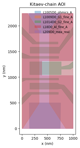
4. Inspect the layout layers
Still at the prepared-layout stage, this AOI plot confirms the cropped DXF window holds the intended source layers before we build the 3D device.
figure = plot_layout_layers(
    prepared.cropped_polygons_by_layer,
    title="Kitaev-chain AOI",
    coordinate_scale=nm_per_unit,
    axis_unit="nm",
)
plt.show()
plt.close(figure)
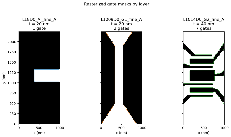
5. Inspect the rasterized masks
Still no Device yet — we are checking the masks that will become gates. Each
panel shows one source layer with all of its disconnected gates overlaid.
figure = plot_gate_stencil_layers(
    prepared.gate_stencils,
    roi_size=prepared.roi_size,
    layer_order=selected_layers,
    title="Rasterized gate masks by layer",
    figsize=(10.8, 5.6),
    coordinate_scale=nm_per_unit,
    axis_unit="nm",
    layer_thicknesses={
        layer["source_layer"]: layer["thickness"]
        for layer in stack
        if layer["kind"] == "gate"
    },
)
plt.show()
plt.close("all")
6. Build the Device
build_device(...) consumes the prepared masks and returns a finalized Device.
# build_device(...) consumes the masks and finalizes the 3D layer geometry.
device = build_device(prepared, stack)

print(format_device_dimensions(device, prepared))
Device summary:
  Lx: 50.0
  Ly: 112.0
  grid: 1.0
  grid_shape: (ny=112, nx=50)
  grid_points: 5600
  layers: buffer, quantum_region, gate_L18D0_Al_fine_A_0, blanket_1, gate_L1009D0_G1_fine_A_0, gate_L1009D0_G1_fine_A_1, blanket_2, gate_L1014D0_G2_fine_A_0, gate_L1014D0_G2_fine_A_1, gate_L1014D0_G2_fine_A_2, gate_L1014D0_G2_fine_A_3, gate_L1014D0_G2_fine_A_4, gate_L1014D0_G2_fine_A_5, gate_L1014D0_G2_fine_A_6
  physical_size: (1e-06 m (1.0 um), 2.24e-06 m (2.24 um))
  grid_constant: 2e-08 m (0.02 um)


/tmp/ipykernel_1558/1219750414.py:2: UserWarning: gate_L18D0_Al_fine_A expands from one stack entry into gate layers ['gate_L18D0_Al_fine_A_0'] from source_layer 'L18D0_Al_fine_A'.
  device = build_device(prepared, stack)
/tmp/ipykernel_1558/1219750414.py:2: UserWarning: gate_L1009D0_G1_fine_A expands from one stack entry into gate layers ['gate_L1009D0_G1_fine_A_0', 'gate_L1009D0_G1_fine_A_1'] from source_layer 'L1009D0_G1_fine_A'.
  device = build_device(prepared, stack)
/tmp/ipykernel_1558/1219750414.py:2: UserWarning: gate_L1014D0_G2_fine_A expands from one stack entry into gate layers ['gate_L1014D0_G2_fine_A_0', 'gate_L1014D0_G2_fine_A_1', 'gate_L1014D0_G2_fine_A_2', 'gate_L1014D0_G2_fine_A_3', 'gate_L1014D0_G2_fine_A_4', 'gate_L1014D0_G2_fine_A_5', 'gate_L1014D0_G2_fine_A_6'] from source_layer 'L1014D0_G2_fine_A'.
  device = build_device(prepared, stack)
7. Mesh the device and solve the electrostatics problem
# Build the pescado problem directly from the finalized per-layer resolutions.
problem_builder = build_problem(
    device,
    vacuum_scale=2.0,
    verbose=False,
)
problem = problem_builder.finalized()
region_shapes = problem.regions_shapes
gate_names = [name for name in problem.regions["dirichlet"] if name != "Boundary"]

# Solve one basis potential per gate.
basis_potentials = solve_gate_potentials(
    problem,
    rhs_block_size=1,
    verbose=False,
)
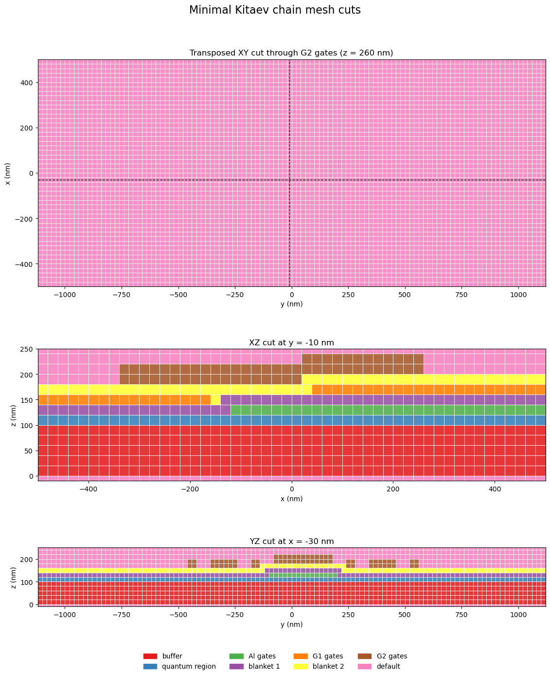
8. Inspect the mesh
Each solved gate carries its own name, but a voltage state reads more naturally when grouped by source layer. The helper below maps a gate back to its layer voltage; we will reuse it in the next step.
def layer_voltage_for_gate(gate_name: str, layer_voltages: dict[str, float]) -> float:
    """Return the grouped source-layer voltage assigned to one solved gate."""
    for source_layer, voltage in layer_voltages.items():
        if gate_name.startswith(f"gate_{source_layer}"):
            return float(voltage)
    return 0.0
Three stacked cuts through the finalized mesh: a transposed xy plane through
the patterned G2 layer at z = 260 nm, a central xz cut, and a yz cut just
left of center.
plot_region_shapes = dict(region_shapes)
plot_region_shapes.pop("Boundary", None)

region_display_names = {}
for region_name in region_shapes:
    if region_name.startswith("gate_L18D0_Al_fine_A"):
        region_display_names[region_name] = "Al gates"
    elif region_name.startswith("gate_L1009D0_G1_fine_A"):
        region_display_names[region_name] = "G1 gates"
    elif region_name.startswith("gate_L1014D0_G2_fine_A"):
        region_display_names[region_name] = "G2 gates"

coordinates = np.asarray(problem.coordinates, dtype=float)
x_cut = nearest_axis_value(coordinates, 0, -1.0)
y_cut = nearest_axis_value(coordinates, 1, 0.0)
mesh_xy_z = 13.0
mesh_plane_specs = make_standard_plane_specs(
    device,
    xy_title=f"XY cut through G2 gates (z = {mesh_xy_z * nm_per_unit:.0f} nm)",
    xy_plane_z=mesh_xy_z,
    xz_title=f"XZ cut at y = {y_cut * nm_per_unit:.0f} nm",
    xz_plane_y=y_cut,
    yz_title=f"YZ cut at x = {x_cut * nm_per_unit:.0f} nm",
    yz_plane_x=x_cut,
)
mesh_plane_specs["XY"] = transpose_plane_spec(
    mesh_plane_specs["XY"],
    title=f"Transposed XY cut through G2 gates (z = {mesh_xy_z * nm_per_unit:.0f} nm)",
)
plane_axes = [mesh_plane_specs["XY"], mesh_plane_specs["XZ"], mesh_plane_specs["YZ"]]
figure, axes = make_xy_emphasis_axes(
    figsize=(11.2, 13.8),
    layout="stack",
    height_ratios=(2.0, 1.1, 0.9),
)

figure, _ = plot_problem_regions_with_mesh(
    problem,
    plot_region_shapes,
    plane_axes,
    axes=axes,
    region_display_names=region_display_names,
    suptitle="Minimal Kitaev chain mesh cuts",
    show_volume_edges=True,
    show_mesh_points=False,
    tile_edgecolors="#f3f3f3",
    coordinate_scale=nm_per_unit,
    axis_unit="nm",
)
add_plane_cut_guides(axes[0], x=y_cut, y=x_cut, coordinate_scale=nm_per_unit)
plt.show()
plt.close(figure)
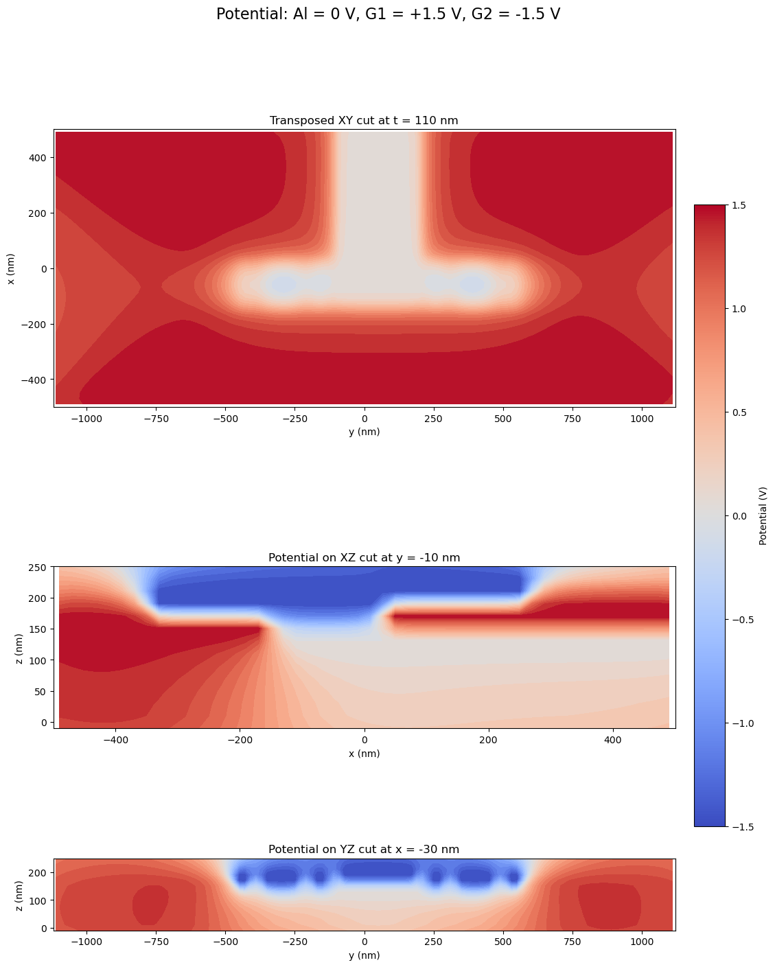
9. A dot-like configuration in the quantum region plane
Now apply a voltage state and look at the potential in the quantum region. Grouping the
basis fields by source layer, the combination below carves two dot-like islands
along the G2-defined chain — the building block of a minimal Kitaev chain.
potential_vmin and potential_vmax set the displayed color scale.
layer_voltages = {
    "L18D0_Al_fine_A": 0.0,
    "L1009D0_G1_fine_A": 1.5,
    "L1014D0_G2_fine_A": -1.5,
}
potential_vmin = -1.5
potential_vmax = 1.5
combined_field = np.zeros(problem.coordinates.shape[0], dtype=float)
for gate_name in gate_names:
    combined_field += layer_voltage_for_gate(gate_name, layer_voltages) * basis_potentials[gate_name]
potential_xy_z = nearest_axis_value(
    coordinates,
    2,
    float(np.asarray(device.layers["quantum_region"].shape.bbox, dtype=float)[1, 2]),
)
potential_plane_specs = make_standard_plane_specs(
    device,
    xy_title=f"Potential on XY cut at t = {potential_xy_z * nm_per_unit:.0f} nm",
    xy_plane_z=potential_xy_z,
    xz_title=f"Potential on XZ cut at y = {y_cut * nm_per_unit:.0f} nm",
    xz_plane_y=y_cut,
    yz_title=f"Potential on YZ cut at x = {x_cut * nm_per_unit:.0f} nm",
    yz_plane_x=x_cut,
)
potential_plane_specs["XY"] = transpose_plane_spec(
    potential_plane_specs["XY"],
    title=f"Transposed XY cut at t = {potential_xy_z * nm_per_unit:.0f} nm",
)

fig, axes = make_xy_emphasis_axes(
    figsize=(11.2, 14.6),
    layout="stack",
    height_ratios=(2.0, 1.1, 0.9),
)
fig, axes = plot_scalar_field_on_planes(
    problem,
    combined_field,
    [
        potential_plane_specs["XY"],
        potential_plane_specs["XZ"],
        potential_plane_specs["YZ"],
    ],
    axes=axes,
    suptitle="Potential: Al = 0 V, G1 = +1.5 V, G2 = -1.5 V",
    colorbar_label="Potential (V)",
    vmin=potential_vmin,
    vmax=potential_vmax,
    symmetric=potential_vmin is None and potential_vmax is None,
    coordinate_scale=nm_per_unit,
    axis_unit="nm",
)
print(format_mapping_block("Layer voltages", layer_voltages, value_formatter=format_voltage))
plt.show()
plt.close(fig)
Layer voltages:
  L18D0_Al_fine_A: +0.00 V
  L1009D0_G1_fine_A: +1.50 V
  L1014D0_G2_fine_A: -1.50 V