Triple Quantum Dot
This is the recommended first read. We take a real GDS file for a triple quantum
dot, crop the active region, give it a physical scale, build the layered device,
solve the gate response, and look at the potential in the quantum region plane — the
plane where the three dots are confined.
The whole thing is three moves:
- pick the part of the chip to model and set its physical scale;
- describe the heterostructure and gate stack above that layout;
- mesh the device and solve the Poisson problem.
For the logic and math behind each step — the layout workflow, the meshing, and the gate-basis solve — see the per-file API Reference.
Worked example
1. Read the GDS file and pick the source layers
First, open the layout and note the source-layer names you want to carry into
the device. (The whole-chip and interactive views come from
layout.extraction; here we start once the gate
layers are already identified.)
from pathlib import Path

import matplotlib.pyplot as plt
import numpy as np

from tempura import build_device, build_problem, prepare_layout, solve_gate_potentials
from tempura.electrostatics import extract_quantum_region_plane
from tempura.formatting import format_mapping_block, format_sequence_inline, format_voltage
from tempura.layout import (
    format_device_dimensions,
    format_roi_summary,
    make_aoi_bbox_from_ranges,
    plot_gate_stencil_layers,
    plot_layout_layers,
)
from tempura.plotting import (
    make_xy_emphasis_axes,
    make_standard_plane_specs,
    nearest_axis_value,
    plot_problem_regions_with_mesh,
    plot_scalar_field_on_planes,
)

selected_source_layers = ["L4D2", "L5D2"]
2. Choose the AOI and the length scale
The AOI is still in the original GDS coordinates. grid_constant_m sets what one
internal Tempura unit means in meters after rasterization — here, 10 nm.
# The AOI is still expressed in the original GDS coordinate system.
aoi_bbox = make_aoi_bbox_from_ranges(
    x_range=(-2170.4, -2169.6),
    y_range=(1569.75, 1570.25),
)

# One internal XY unit will correspond to 10 nm after prepare_layout(...).
grid_constant_m = 10e-9
nm_per_unit = grid_constant_m * 1e9
From here on, lengths are in grid units
After prepare_layout(...), Tempura works in internal units, not meters.
With grid_constant_m = 10e-9, one unit is 10 nm, and the AOI size,
device.length, device.width, gate masks, layer thicknesses, and every
resolution=[dx, dy, dz] are all in those units. The physical ROI must be an
integer number of grid cells.
3. Define the vertical stack
With the lateral layout fixed, the remaining physical input is the stack, written
bottom-to-top: where the QuantumRegion sits, which dielectrics separate it from the
metal, and which source layers become gates.
# The stack is the physical device specification, written bottom-to-top.
stack = [
    {
        "kind": "dielectric",
        "name": "buffer",
        "permittivity": 12.9,
        "thickness": 10.0,
    },
    {
        "kind": "quantum_region",
        "name": "quantum_region",
        "permittivity": 12.9,
        "thickness": 2.0,
    },
    {
        "kind": "dielectric",
        "name": "blanket_0",
        "permittivity": 9.1,
        "thickness": 1.0,
    },
    {
        "kind": "gate",
        "name": f"gate_{selected_source_layers[0]}",
        "source_layer": selected_source_layers[0],
        "thickness": 2.0,
    },
    {
        "kind": "dielectric",
        "name": "blanket_1",
        "permittivity": 9.1,
        "thickness": 1.0,
    },
    {
        "kind": "gate",
        "name": f"gate_{selected_source_layers[1]}",
        "source_layer": selected_source_layers[1],
        "thickness": 2.0,
    },
]
A single gate entry can become several Gate objects: if its source layer
rasterizes to multiple disconnected masks, Tempura emits one gate per mask and
suffixes the names automatically.
4. Prepare the layout
prepare_layout(...) crops the AOI, rescales it into internal units, and
rasterizes the selected source layers onto the device grid.
# This is the layout handoff into Tempura's internal grid units.
prepared = prepare_layout(
    layout_path=layout_path,
    aoi_bbox=aoi_bbox,
    size_mode="layout_size",
    grid_constant_m=grid_constant_m,
)

available_selected_source_layers = [
    layer_name
    for layer_name in selected_source_layers
    if layer_name in prepared.gate_stencils
]
print(format_sequence_inline("Selected layers", available_selected_source_layers))
print(format_roi_summary(prepared))
Selected layers: L4D2, L5D2
ROI summary:
  physical_size: (8e-07 m (0.8 um), 5e-07 m (0.5 um))
  grid_constant: 1e-08 m (0.01 um)
  rescaled_size: (80.0, 50.0)
  grid_shape: (ny=50, nx=80)
  grid_points: 4000
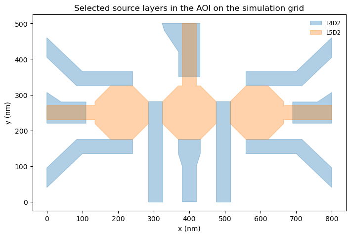
5. Check the layers landed in the AOI
Before building the 3D device, confirm the cropped AOI still holds the expected layers after rescaling onto the simulation grid.
figure = plot_layout_layers(
    prepared.cropped_polygons_by_layer,
    layers=available_selected_source_layers,
    title="Selected source layers in the AOI on the simulation grid",
    coordinate_scale=nm_per_unit,
    axis_unit="nm",
)
plt.show()
plt.close(figure)
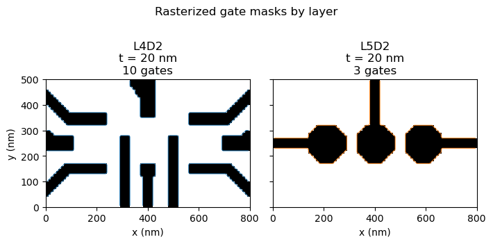
6. Check the gate masks
This is the best moment to catch a wrong AOI, a bad scale, or an unwanted layer — before the 3D device exists. Each panel shows one source layer with all of its disconnected gates overlaid.
figure = plot_gate_stencil_layers(
    prepared.gate_stencils,
    roi_size=prepared.roi_size,
    layer_order=available_selected_source_layers,
    title="Rasterized gate masks by layer",
    coordinate_scale=nm_per_unit,
    axis_unit="nm",
    layer_thicknesses={
        layer["source_layer"]: layer["thickness"]
        for layer in stack
        if layer["kind"] == "gate"
    },
)
plt.show()
plt.close("all")
7. Build the device
build_device(...) combines the rasterized masks with the vertical stack and
returns a finalized Device, ready for meshing.
# build_device(...) consumes the rasterized masks and finalizes the geometry.
device = build_device(prepared, stack)

print(format_device_dimensions(device, prepared))
Device summary:
  Lx: 80.0
  Ly: 50.0
  grid: 1.0
  grid_shape: (ny=50, nx=80)
  grid_points: 4000
  layers: buffer, quantum_region, blanket_0, gate_L4D2_0, gate_L4D2_1, gate_L4D2_2, gate_L4D2_3, gate_L4D2_4, gate_L4D2_5, gate_L4D2_6, gate_L4D2_7, gate_L4D2_8, gate_L4D2_9, blanket_1, gate_L5D2_0, gate_L5D2_1, gate_L5D2_2
  physical_size: (8e-07 m (0.8 um), 5e-07 m (0.5 um))
  grid_constant: 1e-08 m (0.01 um)


/tmp/ipykernel_1578/2419023549.py:2: UserWarning: gate_L4D2 expands from one stack entry into gate layers ['gate_L4D2_0', 'gate_L4D2_1', 'gate_L4D2_2', 'gate_L4D2_3', 'gate_L4D2_4', 'gate_L4D2_5', 'gate_L4D2_6', 'gate_L4D2_7', 'gate_L4D2_8', 'gate_L4D2_9'] from source_layer 'L4D2'.
  device = build_device(prepared, stack)
/tmp/ipykernel_1578/2419023549.py:2: UserWarning: gate_L5D2 expands from one stack entry into gate layers ['gate_L5D2_0', 'gate_L5D2_1', 'gate_L5D2_2'] from source_layer 'L5D2'.
  device = build_device(prepared, stack)
8. Mesh and solve
The sample is now fixed, so the rest is numerical: build_problem(...) assembles
a ProblemBuilder, problem_builder.finalized() turns it into the fixed Pescado
problem, and solve_gate_potentials(...) computes one basis response per gate.
# Build the pescado problem directly from the finalized per-layer resolutions.
problem_builder = build_problem(
    device,
    vacuum_scale=2.0,
    verbose=False,
)
problem = problem_builder.finalized()
region_shapes = problem.regions_shapes
gate_names = [name for name in problem.regions["dirichlet"] if name != "Boundary"]

# One source layer can expand into many concrete gates, so keep the solve
# batched instead of forcing a one-gate-at-a-time loop.
rhs_block_size = max(1, min(len(gate_names), 8))

# Solve one basis potential per gate.
basis_potentials = solve_gate_potentials(
    problem,
    rhs_block_size=rhs_block_size,
    verbose=False,
)
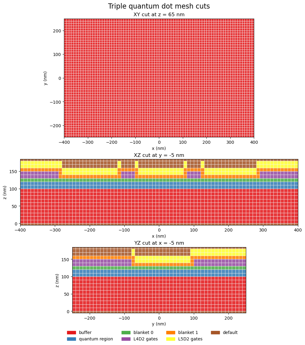
9. Inspect the mesh
Three cuts through the finalized mesh: a horizontal xy plane at z = 70 nm, a
vertical xz plane through the device center, and a vertical yz plane through
the same center line.
plane = extract_quantum_region_plane(problem, region_shapes)

plot_region_shapes = dict(region_shapes)
plot_region_shapes.pop("Boundary", None)

coordinates = np.asarray(problem.coordinates, dtype=float)
x_cut = nearest_axis_value(coordinates, 0, 0.0)
y_cut = nearest_axis_value(coordinates, 1, 0.0)
mesh_xy_z = nearest_axis_value(coordinates, 2, 7.0)
potential_xy_z = nearest_axis_value(
    coordinates,
    2,
    float(np.asarray(device.layers["quantum_region"].shape.bbox, dtype=float)[1, 2]),
)
mesh_plane_specs = make_standard_plane_specs(
    device,
    xy_title=f"XY cut at z = {mesh_xy_z * nm_per_unit:.0f} nm",
    xy_plane_z=mesh_xy_z,
    xz_title=f"XZ cut at y = {y_cut * nm_per_unit:.0f} nm",
    xz_plane_y=y_cut,
    yz_title=f"YZ cut at x = {x_cut * nm_per_unit:.0f} nm",
    yz_plane_x=x_cut,
)
potential_plane_specs = make_standard_plane_specs(
    device,
    xy_title=f"Potential on XY cut at t = {potential_xy_z * nm_per_unit:.0f} nm",
    xy_plane_z=potential_xy_z,
    xz_title=f"Potential on XZ cut at y = {y_cut * nm_per_unit:.0f} nm",
    xz_plane_y=y_cut,
    yz_title=f"Potential on YZ cut at x = {x_cut * nm_per_unit:.0f} nm",
    yz_plane_x=x_cut,
)

region_display_names = {}
for region_name in region_shapes:
    if region_name.startswith(f"gate_{selected_source_layers[0]}"):
        region_display_names[region_name] = f"{selected_source_layers[0]} gates"
    elif region_name.startswith(f"gate_{selected_source_layers[1]}"):
        region_display_names[region_name] = f"{selected_source_layers[1]} gates"

figure, axes = make_xy_emphasis_axes(
    figsize=(15.2, 11.2),
    height_ratios=(1.8, 1.0, 1.0),
)
figure, _ = plot_problem_regions_with_mesh(
    problem,
    plot_region_shapes,
    [mesh_plane_specs["XY"], mesh_plane_specs["XZ"], mesh_plane_specs["YZ"]],
    axes=axes,
    region_display_names=region_display_names,
    suptitle="Triple quantum dot mesh cuts",
    show_volume_edges=True,
    show_mesh_points=False,
    tile_edgecolors="#f3f3f3",
    coordinate_scale=nm_per_unit,
    axis_unit="nm",
)
plt.show()
plt.close(figure)
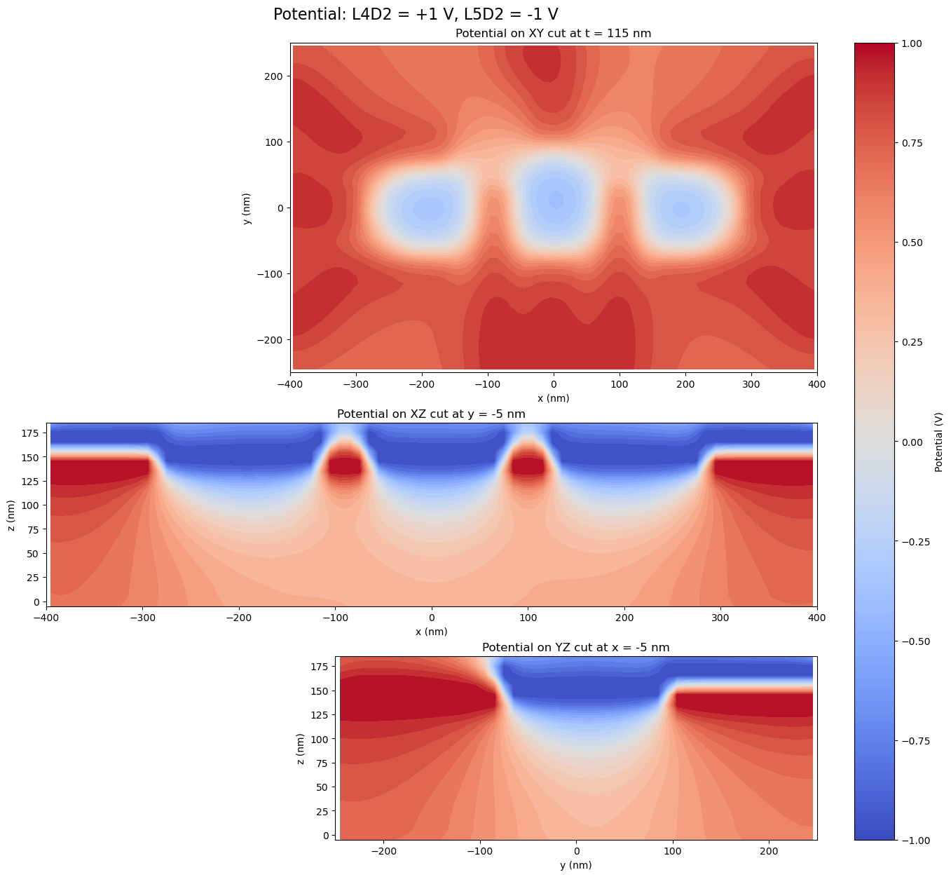
10. Apply a gate configuration
The payoff: because the solve is linear, any voltage configuration is a weighted
sum of the basis responses — no resolve needed. Here we set every gate from the
first source layer to +1 V and every gate from the second to -1 V, then read
the resulting potential in the quantum region plane.
gate_voltages = {}
combined_potential = np.zeros(problem.coordinates.shape[0], dtype=float)
for gate_name in gate_names:
    if gate_name.startswith(f"gate_{selected_source_layers[0]}"):
        voltage = 1.0
    else:
        voltage = -1.0
    gate_voltages[gate_name] = voltage
    combined_potential += voltage * basis_potentials[gate_name]

fig, axes = make_xy_emphasis_axes(
    figsize=(15.2, 12.4),
    height_ratios=(1.8, 1.0, 1.0),
)
fig, axes = plot_scalar_field_on_planes(
    problem,
    combined_potential,
    [
        potential_plane_specs["XY"],
        potential_plane_specs["XZ"],
        potential_plane_specs["YZ"],
    ],
    axes=axes,
    suptitle=(
        f"Potential: {selected_source_layers[0]} = +1 V, "
        f"{selected_source_layers[1]} = -1 V"
    ),
    colorbar_label="Potential (V)",
    coordinate_scale=nm_per_unit,
    axis_unit="nm",
)
print(format_mapping_block("Gate voltages", gate_voltages, value_formatter=format_voltage))
plt.show()
plt.close(fig)
Gate voltages:
  gate_L4D2_0: +1.00 V
  gate_L4D2_1: +1.00 V
  gate_L4D2_2: +1.00 V
  gate_L4D2_3: +1.00 V
  gate_L4D2_4: +1.00 V
  gate_L4D2_5: +1.00 V
  gate_L4D2_6: +1.00 V
  gate_L4D2_7: +1.00 V
  gate_L4D2_8: +1.00 V
  gate_L4D2_9: +1.00 V
  gate_L5D2_0: -1.00 V
  gate_L5D2_1: -1.00 V
  gate_L5D2_2: -1.00 V