Device, Mesh, and Solve
This page shows the core Tempura modeling chain without going through a layout
file. The starting point is a layered sample: a lateral gate pattern in the
xy plane, a vertical stack of metals and dielectrics along z, and a
TwoDEG whose electrostatic environment we want to model.
The goal is to see how Device, per-layer resolution, build_problem(...),
and solve_gate_potentials(...) fit together. For the full layout-backed
workflow, see Triple Quantum Dot. For generated
signatures, see API Reference.
Worked Example
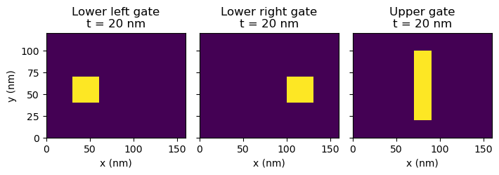
1. Define the lateral gate geometry
The Device starts with a simulation window in the plane. Inside that window,
each gate is represented by a stencil on a regular square lattice.
import matplotlib.pyplot as plt
import numpy as np

from tempura import Device, Dielectric, Gate, TwoDEG
from tempura.electrostatics import build_problem, solve_gate_potentials
from tempura.plotting import (
    add_plane_cut_guides,
    make_xy_emphasis_axes,
    make_standard_plane_specs,
    nearest_axis_value,
    plot_problem_regions_with_mesh,
    plot_scalar_field_on_planes,
    transpose_plane_spec,
)

nm_per_unit = 10.0

length = 16.0
width = 12.0
grid = 1.0

device = Device(length=length, width=width, grid=grid)
grid_shape = device.grid_shape


def rect_mask(
    shape: tuple[int, int],
    *,
    row_start: int,
    row_stop: int,
    col_start: int,
    col_stop: int,
) -> np.ndarray:
    """Return one rectangular gate mask on the device lattice."""
    mask = np.zeros(shape, dtype=bool)
    mask[row_start:row_stop, col_start:col_stop] = True
    return mask


lower_left = rect_mask(grid_shape, row_start=4, row_stop=7, col_start=3, col_stop=6)
lower_right = rect_mask(grid_shape, row_start=4, row_stop=7, col_start=10, col_stop=13)
upper_gate = rect_mask(grid_shape, row_start=2, row_stop=10, col_start=7, col_stop=9)
fig, ax = plt.subplots(ncols=3, figsize=(7.2, 2.4), sharex=True, sharey=True)
ax[0].imshow(lower_left, origin="lower", extent=(0, length * nm_per_unit, 0, width * nm_per_unit), vmin=0)
ax[0].set_title("Lower left gate\nt = 20 nm")
ax[0].set_xlabel("x (nm)")
ax[0].set_ylabel("y (nm)")
ax[1].imshow(lower_right, origin="lower", extent=(0, length * nm_per_unit, 0, width * nm_per_unit), vmin=0)
ax[1].set_title("Lower right gate\nt = 20 nm")
ax[1].set_xlabel("x (nm)")
ax[2].imshow(upper_gate, origin="lower", extent=(0, length * nm_per_unit, 0, width * nm_per_unit), vmin=0)
ax[2].set_title("Upper gate\nt = 20 nm")
ax[2].set_xlabel("x (nm)")
plt.tight_layout()
2. Build the vertical stack
The next step is the vertical stack itself: substrate, TwoDEG, dielectric
spacers, and metal layers. Layers are added in bottom-to-top order because that
order defines the final geometry.
This example also requests a finer vertical mesh in the TwoDEG through
resolution=[grid, grid, 0.5]. With nm_per_unit = 10, that keeps the
in-plane lattice at 10 nm while refining the master dz to 5 nm.
Stacking rules that matter
- Add layers in bottom-to-top order.
- Gates deposited together should be passed as one batch with
device.add_layer([...]). - Every gate stencil must match
device.grid_shape.
device.add_layer(
    Dielectric(
        name="substrate",
        permittivity=12.9,
        thickness=8.0,
    )
)
device.add_layer(
    TwoDEG(
        name="2deg",
        permittivity=12.9,
        thickness=1.0,
        resolution=[grid, grid, 0.25],
    )
)
device.add_layer(
    Dielectric(
        name="barrier_0",
        permittivity=9.1,
        thickness=1.0,
    )
)
device.add_layer(
    [
        Gate(
            name="lower_left",
            thickness=2.0,
            stencil=lower_left,
        ),
        Gate(
            name="lower_right",
            thickness=2.0,
            stencil=lower_right,
        ),
    ]
)
device.add_layer(
    Dielectric(
        name="barrier_1",
        permittivity=9.1,
        thickness=1.0,
    )
)
device.add_layer(
    Gate(
        name="upper_gate",
        thickness=2.0,
        stencil=upper_gate,
    )
)
device.finalize()
What finalize() does
finalize() is the boundary between an editable stack specification and
derived geometry. After that call, Tempura has built height fields and 3D
shapes for every layer, and the layer inputs are treated as fixed.
3. Build the meshed Poisson problem
Geometry and discretization are separate. Each layer can request its own
resolution=[dx, dy, dz], but the TwoDEG defines the finest master lattice.
Coarser requests are rounded up to commensurate multiples when necessary so the
final mesh stays aligned.
Resolution rule
The TwoDEG resolution must match the exact device XY grid. Other layer
resolutions are resolved onto that lattice during build_problem(...).
Here the TwoDEG sets dx = dy = 1 and a finer master dz = 0.5.
The device halo and the finer TwoDEG slab are separate
Tempura first builds an aligned halo around the full realized device stack
using the smallest non-TwoDEG lattice spacing. If the TwoDEG asks for
a finer dz, that extra refinement is then applied only inside the
TwoDEG slab itself.
Default TwoDEG resolution can be a footgun
Layers without an explicit resolution default to [1, 1, 1]. That is
coarser than the mesh used in this example. If your device uses a different
XY grid spacing, or if you want a finer vertical mesh in the TwoDEG, set
TwoDEG(resolution=[grid, grid, dz]) explicitly.
problem_builder, region_shapes, gate_names = build_problem(device, vacuum_scale=2.0)
problem = problem_builder.finalized()
build_problem(...) turns the finalized device into solver-owned regions.
region_shapes tells you which parts of the final mesh belong to each physical
layer, while gate_names defines the order used later in the basis solve.
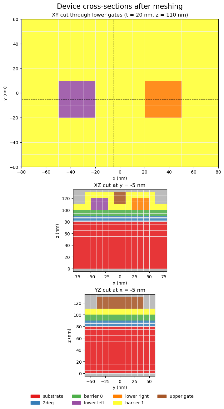
4. Inspect the final mesh
The easiest way to understand the mesh is to cut through it. The plots below show one transposed horizontal slice through the lower gates and two vertical slices through the stack. The colored regions are the final solver-owned regions; the overlay shows the control-volume edges used by the discretization.
coordinates = np.asarray(problem.coordinates, dtype=float)
lower_gate_bbox = np.asarray(device.layers["lower_left"].shape.bbox, dtype=float)
lower_gate_mid_z = float(0.5 * (lower_gate_bbox[0, 2] + lower_gate_bbox[1, 2]))
lower_gate_plane_z = nearest_axis_value(coordinates, 2, lower_gate_mid_z)
y_cut = nearest_axis_value(coordinates, 1, 0.0)
x_cut = nearest_axis_value(coordinates, 0, 0.0)
plane_specs = make_standard_plane_specs(
    device,
    xy_title=f"XY cut through lower gates (t = 20 nm, z = {lower_gate_plane_z * nm_per_unit:.0f} nm)",
    xy_plane_z=lower_gate_plane_z,
    xz_title=f"XZ cut at y = {y_cut * nm_per_unit:.0f} nm",
    xz_plane_y=y_cut,
    yz_title=f"YZ cut at x = {x_cut * nm_per_unit:.0f} nm",
    yz_plane_x=x_cut,
)

figure, axes = make_xy_emphasis_axes(
    figsize=(11.2, 13.0),
    layout="stack",
    height_ratios=(1.8, 1.0, 1.0),
)

figure, axes = plot_problem_regions_with_mesh(
    problem,
    region_shapes,
    [plane_specs["XY"], plane_specs["XZ"], plane_specs["YZ"]],
    axes=axes,
    suptitle="Device cross-sections after meshing",
    show_volume_edges=True,
    show_mesh_points=False,
    tile_edgecolors="#f3f3f3",
    tile_linewidth=0.5,
    coordinate_scale=nm_per_unit,
    axis_unit="nm",
)
add_plane_cut_guides(axes[0], x=y_cut, y=x_cut, coordinate_scale=nm_per_unit)
5. Solve the gate basis
With a fixed geometry and a fixed mesh, Tempura's default solve computes one basis potential per gate. Each basis solution answers the question: what does the electrostatic potential look like if this gate is at unit voltage and the others are grounded?
basis_potentials, problem = solve_gate_potentials(
    problem_builder,
    region_shapes,
    gate_names,
    rhs_block_size=1,
)

gate_voltages = {"lower_left": -1.0, "lower_right": -1.0, "upper_gate": 2.0}
combined_potential = np.zeros(problem.coordinates.shape[0], dtype=float)
for gate_name in gate_names:
    combined_potential += gate_voltages[gate_name] * basis_potentials[gate_name]

potential_xy_z = nearest_axis_value(
    coordinates,
    2,
    float(np.asarray(device.layers["2deg"].shape.bbox, dtype=float)[1, 2]),
)
potential_plane_specs = make_standard_plane_specs(
    device,
    xy_title=f"Potential on XY cut at t = {potential_xy_z * nm_per_unit:.0f} nm",
    xy_plane_z=potential_xy_z,
    xz_title=f"Potential on XZ cut at y = {y_cut * nm_per_unit:.0f} nm",
    xz_plane_y=y_cut,
    yz_title=f"Potential on YZ cut at x = {x_cut * nm_per_unit:.0f} nm",
    yz_plane_x=x_cut,
)
potential_plane_specs["XY"] = transpose_plane_spec(
    potential_plane_specs["XY"],
    title=f"Transposed XY cut at t = {potential_xy_z * nm_per_unit:.0f} nm",
)
fig, axes = make_xy_emphasis_axes(
    figsize=(11.2, 13.6),
    layout="stack",
    height_ratios=(1.8, 1.0, 1.0),
)
fig, axes = plot_scalar_field_on_planes(
    problem,
    combined_potential,
    [
        potential_plane_specs["XY"],
        potential_plane_specs["XZ"],
        potential_plane_specs["YZ"],
    ],
    axes=axes,
    suptitle="Potential: lower gates = +1 V, upper gate = -1 V",
    colorbar_label="Potential (V)",
    coordinate_scale=nm_per_unit,
    axis_unit="nm",
    vmin=-1, vmax=1
)
plt.show()
plt.close(fig)
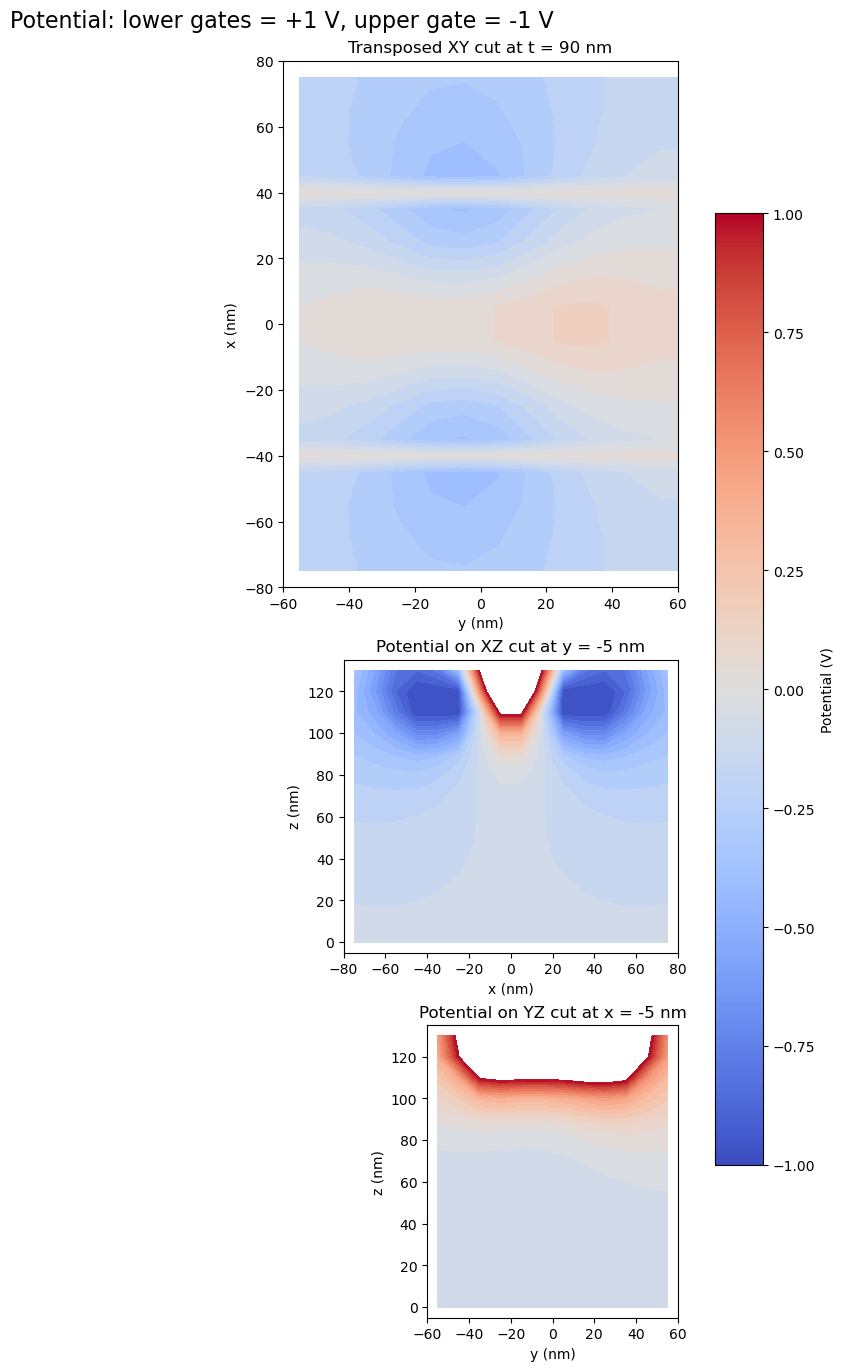
The exact values depend on the geometry and mesh, but the important point is that the solve returns one field per gate, keyed by gate name. Later voltage configurations can be assembled from linear combinations of those basis fields.
What solve_gate_potentials(...) returns
Each entry in basis_potentials is a full solver vector, not an already
reshaped xy array. The worked examples use extract_2deg_plane(...) and
extract_2deg_basis(...) when they want a rectangular 2DEG view for
plotting.
Interpretation
The core Tempura workflow is:
- describe the physical stack with
Device,Gate,Dielectric, andTwoDEG; - call
finalize()to derive the geometry; - assign or accept per-layer
resolution=[dx, dy, dz]; - call
build_problem(...)to assemble the meshed Poisson problem; - call
solve_gate_potentials(...)to compute the gate basis.
For self-consistent TwoDEG problems, the next step is TFSolver. For the
mathematical background, see Theory. For the layout-backed
version of the same pipeline, see Triple Quantum Dot.