Triple Quantum Dot
This example takes a real GDS file for a triple quantum dot, crops one active region, assigns it a physical scale, builds the layered device, solves the electrostatic gate response, and inspects the result in the 2DEG plane.
The workflow has three parts:
- choose the part of the chip to model and assign its physical scale;
- define the vertical heterostructure and gate stack above that layout;
- mesh the finalized device and solve the Poisson problem.
For the supporting concept pages, see Layout, Device, Mesh, and Solve, and Theory. For generated signatures, see API Reference.
Worked Example
1. Read the GDS file and choose the source layers
The first step is to inspect the layout file and record the source-layer names that should be carried into the device model.
from pathlib import Path

import matplotlib.pyplot as plt
import numpy as np

from tempura.electrostatics.pescado_wrapper import (
    build_problem,
    extract_2deg_plane,
    solve_gate_potentials,
)
from tempura.formatting import format_mapping_block, format_sequence_inline, format_voltage
from tempura.layout.extraction import (
    make_aoi_bbox_from_ranges,
    plot_gate_stencil_layers,
    plot_layout_layers,
)
from tempura.layout.layout_pipeline import (
    build_device,
    format_device_dimensions,
    format_roi_summary,
    prepare_layout,
)
from tempura.plotting import (
    make_xy_emphasis_axes,
    make_standard_plane_specs,
    nearest_axis_value,
    plot_problem_regions_with_mesh,
    plot_scalar_field_on_planes,
)

selected_source_layers = ["L4D2", "L5D2"]
The whole-chip interactive inspection step lives on Layout. This page starts from the point where the relevant source layers have already been identified.
2. Choose the AOI and internal length scale
The AOI is still expressed in the original GDS coordinate system. grid_constant_m
sets the physical size of one internal Tempura unit after rasterization.
# The AOI is still expressed in the original GDS coordinate system.
aoi_bbox = make_aoi_bbox_from_ranges(
    x_range=(-2170.4, -2169.6),
    y_range=(1569.75, 1570.25),
)

# One internal XY unit will correspond to 10 nm after prepare_layout(...).
grid_constant_m = 10e-9
nm_per_unit = grid_constant_m * 1e9
Units after prepare_layout(...)
Tempura does not keep working in meters after the layout is rasterized. If
grid_constant_m = 10e-9, then one internal unit is 10 nm. From that
point on, the cropped AOI size, device.length, device.width, gate
masks, layer thicknesses, and every layer resolution=[dx, dy, dz] are all
expressed in those internal units. The physical ROI dimensions therefore
need to be integer multiples of grid_constant_m.
3. Define the vertical stack
Once the lateral layout is fixed, the remaining physical input is the ordered
stack: where the TwoDEG sits, what dielectric layers separate it from the
metal, and which source layers become gates.
# The stack is the physical device specification, written bottom-to-top.
stack = [
    {
        "kind": "dielectric",
        "name": "buffer",
        "permittivity": 12.9,
        "thickness": 4.0,
    },
    {
        "kind": "2deg",
        "name": "2deg",
        "permittivity": 12.9,
        "thickness": 1.0,
    },
    {
        "kind": "dielectric",
        "name": "blanket_0",
        "permittivity": 9.1,
        "thickness": 1.0,
    },
    {
        "kind": "gate",
        "name": f"gate_{selected_source_layers[0]}",
        "source_layer": selected_source_layers[0],
        "thickness": 2.0,
    },
    {
        "kind": "dielectric",
        "name": "blanket_1",
        "permittivity": 9.1,
        "thickness": 1.0,
    },
    {
        "kind": "gate",
        "name": f"gate_{selected_source_layers[1]}",
        "source_layer": selected_source_layers[1],
        "thickness": 3.0,
    },
]
Note
A single gate stack entry can expand into several Gate objects if the
rasterized source layer contains several non-empty disconnected masks. In
the finalized device, those gates are suffixed automatically.
4. Prepare the layout
prepare_layout(...) crops the AOI, rescales it into Tempura's internal units,
and rasterizes the selected source layers onto the device grid.
# This is the layout handoff into Tempura's internal grid units.
prepared = prepare_layout(
    layout_path=layout_path,
    aoi_bbox=aoi_bbox,
    size_mode="layout_size",
    grid_constant_m=grid_constant_m,
)

available_selected_source_layers = [
    layer_name
    for layer_name in selected_source_layers
    if layer_name in prepared["gate_stencils"]
]
print(format_sequence_inline("Selected layers", available_selected_source_layers))
print(format_roi_summary(prepared))
Selected layers: L4D2, L5D2
ROI summary:
  layout_size: (0.8000000000001819, 0.5)
  physical_size: (8.000000000001819e-07 m (0.8000000000001819 um), 5e-07 m (0.5 um))
  grid_constant: 1e-08 m (0.01 um)
  rescaled_size: (80.0, 50.0)
  grid_shape: (ny=50, nx=80)
  grid_points: 4000
  layout_unit_scale: 1e-06 m (1.0 um)
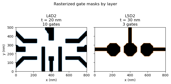
5. Check the masks that will feed build_device(...)
This is usually the best point to catch a wrong AOI, a bad scale choice, or an unwanted source layer before the full 3D device is built. Each panel below shows one source layer with all disconnected gates from that layer overlaid.
figure = plot_gate_stencil_layers(
    prepared["gate_stencils"],
    roi_size=prepared["roi_size"],
    layer_order=available_selected_source_layers,
    title="Rasterized gate masks by layer",
    coordinate_scale=nm_per_unit,
    axis_unit="nm",
    layer_thicknesses={
        layer["source_layer"]: layer["thickness"]
        for layer in stack
        if layer["kind"] == "gate"
    },
)
plt.show()
plt.close("all")
6. Build the finalized device
build_device(...) combines the layout-backed masks with the vertical stack.
The returned Device is already finalized and ready for meshing.
# build_device(...) consumes the rasterized masks and finalizes the geometry.
device = build_device(prepared, stack)

print(format_device_dimensions(device, prepared))
Device summary:
  Lx: 80.0
  Ly: 50.0
  grid: 1.0
  grid_shape: (ny=50, nx=80)
  grid_points: 4000
  layers: buffer, 2deg, blanket_0, gate_L4D2_0, gate_L4D2_1, gate_L4D2_2, gate_L4D2_3, gate_L4D2_4, gate_L4D2_5, gate_L4D2_6, gate_L4D2_7, gate_L4D2_8, gate_L4D2_9, blanket_1, gate_L5D2_0, gate_L5D2_1, gate_L5D2_2
  physical_size: (8.000000000001819e-07 m (0.8000000000001819 um), 5e-07 m (0.5 um))
  grid_constant: 1e-08 m (0.01 um)
  layout_unit_scale: 1e-06 m (1.0 um)
7. Mesh the device and solve the electrostatics problem
Now the physical sample is fixed. The remaining steps are numerical:
build_problem(...) assembles the meshed Poisson problem and
solve_gate_potentials(...) computes one basis response per gate.
# Build the pescado problem directly from the finalized per-layer resolutions.
problem_builder, region_shapes, gate_names = build_problem(
    device,
    vacuum_scale=2.0,
    verbose=False,
)

# Solve one basis potential per gate.
basis_potentials, problem = solve_gate_potentials(
    problem_builder,
    region_shapes,
    gate_names,
    rhs_block_size=1,
    verbose=False,
)
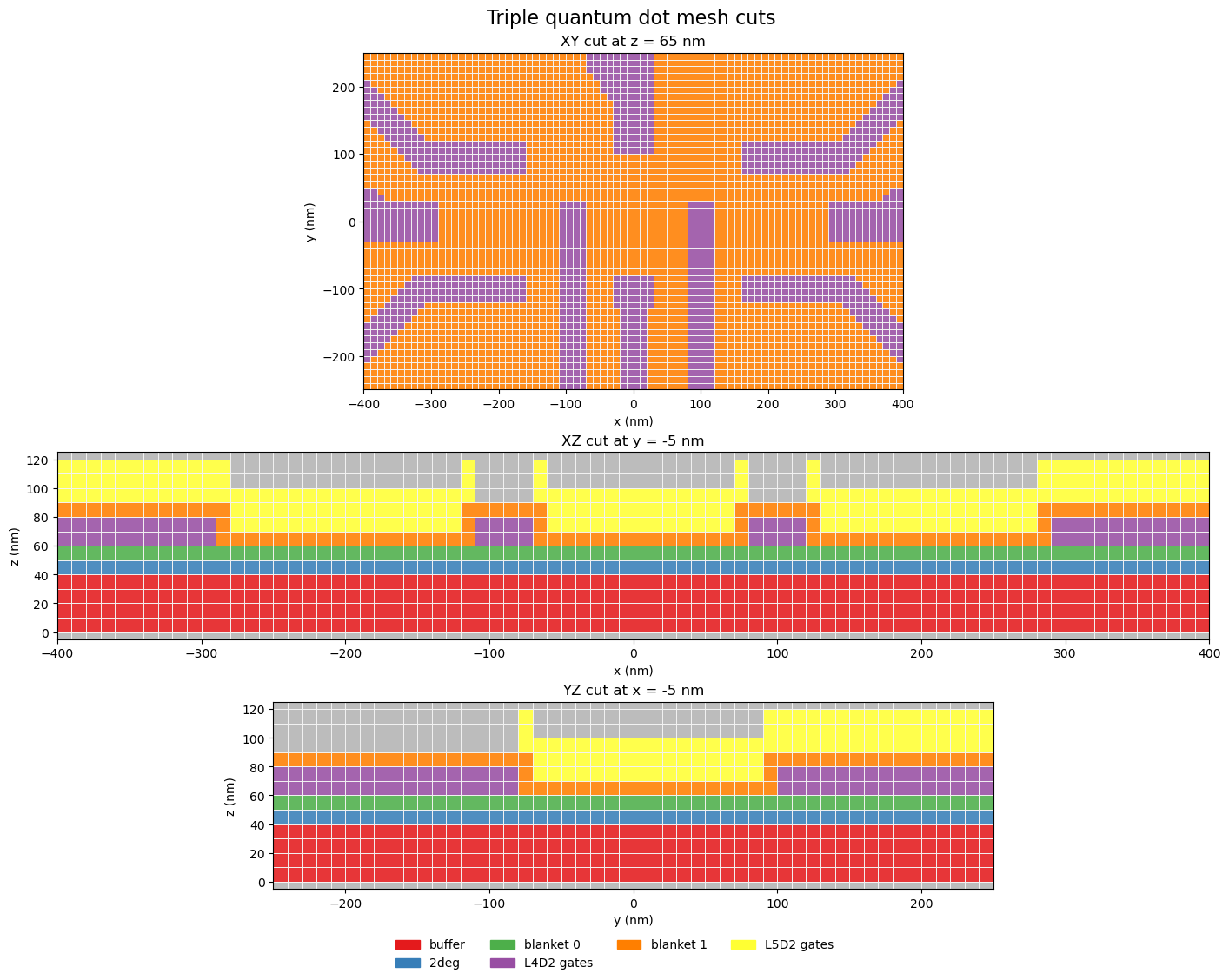
8. Inspect the finalized mesh
The figure below shows three cuts through the finalized Pescado mesh: one
horizontal xy plane at z = 70 nm, one vertical xz plane through the
center of the device, and one vertical yz plane through the same center
line.
plane = extract_2deg_plane(problem, region_shapes)

plot_region_shapes = dict(region_shapes)
plot_region_shapes.pop("Boundary", None)

coordinates = np.asarray(problem.coordinates, dtype=float)
x_cut = nearest_axis_value(coordinates, 0, 0.0)
y_cut = nearest_axis_value(coordinates, 1, 0.0)
mesh_xy_z = nearest_axis_value(coordinates, 2, 7.0)
potential_xy_z = nearest_axis_value(
    coordinates,
    2,
    float(np.asarray(device.layers["2deg"].shape.bbox, dtype=float)[1, 2]),
)
mesh_plane_specs = make_standard_plane_specs(
    device,
    xy_title=f"XY cut at z = {mesh_xy_z * nm_per_unit:.0f} nm",
    xy_plane_z=mesh_xy_z,
    xz_title=f"XZ cut at y = {y_cut * nm_per_unit:.0f} nm",
    xz_plane_y=y_cut,
    yz_title=f"YZ cut at x = {x_cut * nm_per_unit:.0f} nm",
    yz_plane_x=x_cut,
)
potential_plane_specs = make_standard_plane_specs(
    device,
    xy_title=f"Potential on XY cut at t = {potential_xy_z * nm_per_unit:.0f} nm",
    xy_plane_z=potential_xy_z,
    xz_title=f"Potential on XZ cut at y = {y_cut * nm_per_unit:.0f} nm",
    xz_plane_y=y_cut,
    yz_title=f"Potential on YZ cut at x = {x_cut * nm_per_unit:.0f} nm",
    yz_plane_x=x_cut,
)

region_display_names = {}
for region_name in region_shapes:
    if region_name.startswith(f"gate_{selected_source_layers[0]}"):
        region_display_names[region_name] = f"{selected_source_layers[0]} gates"
    elif region_name.startswith(f"gate_{selected_source_layers[1]}"):
        region_display_names[region_name] = f"{selected_source_layers[1]} gates"

figure, axes = make_xy_emphasis_axes(
    figsize=(15.2, 11.2),
    height_ratios=(1.8, 1.0, 1.0),
)
figure, _ = plot_problem_regions_with_mesh(
    problem,
    plot_region_shapes,
    [mesh_plane_specs["XY"], mesh_plane_specs["XZ"], mesh_plane_specs["YZ"]],
    axes=axes,
    region_display_names=region_display_names,
    suptitle="Triple quantum dot mesh cuts",
    show_volume_edges=True,
    show_mesh_points=False,
    tile_edgecolors="#f3f3f3",
    coordinate_scale=nm_per_unit,
    axis_unit="nm",
)
plt.show()
plt.close(figure)
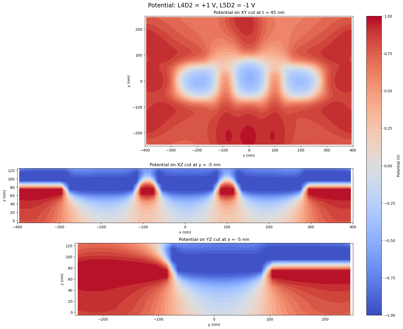
9. Combine one gate configuration in the 2DEG plane
Because the Poisson solve is linear, a physical gate configuration can be
assembled by summing the basis responses with the desired gate voltages. Here
we set every gate from the first source layer to +1 V and every gate from the
second source layer to -1 V.
gate_voltages = {}
combined_potential = np.zeros(problem.coordinates.shape[0], dtype=float)
for gate_name in gate_names:
    if gate_name.startswith(f"gate_{selected_source_layers[0]}"):
        voltage = 1.0
    else:
        voltage = -1.0
    gate_voltages[gate_name] = voltage
    combined_potential += voltage * basis_potentials[gate_name]

fig, axes = make_xy_emphasis_axes(
    figsize=(15.2, 12.4),
    height_ratios=(1.8, 1.0, 1.0),
)
fig, axes = plot_scalar_field_on_planes(
    problem,
    combined_potential,
    [
        potential_plane_specs["XY"],
        potential_plane_specs["XZ"],
        potential_plane_specs["YZ"],
    ],
    axes=axes,
    suptitle=(
        f"Potential: {selected_source_layers[0]} = +1 V, "
        f"{selected_source_layers[1]} = -1 V"
    ),
    colorbar_label="Potential (V)",
    coordinate_scale=nm_per_unit,
    axis_unit="nm",
)
print(format_mapping_block("Gate voltages", gate_voltages, value_formatter=format_voltage))
plt.show()
plt.close(fig)
Gate voltages:
  gate_L4D2_0: +1.00 V
  gate_L4D2_1: +1.00 V
  gate_L4D2_2: +1.00 V
  gate_L4D2_3: +1.00 V
  gate_L4D2_4: +1.00 V
  gate_L4D2_5: +1.00 V
  gate_L4D2_6: +1.00 V
  gate_L4D2_7: +1.00 V
  gate_L4D2_8: +1.00 V
  gate_L4D2_9: +1.00 V
  gate_L5D2_0: -1.00 V
  gate_L5D2_1: -1.00 V
  gate_L5D2_2: -1.00 V