Layout
Layout files provide the lateral metal geometry, but not the full simulation model. Tempura still needs three extra choices:
- which area of interest (AOI) to simulate;
- what physical size that AOI represents;
- how the cropped polygons should be turned into device-aligned masks.
The low-level functions in tempura.layout read polygons, crop an AOI, and
rasterize masks. The higher-level helpers in
tempura.layout.layout_pipeline combine those steps for the common
layout-backed workflow.
For generated signatures, see API Reference.
Most users should start with prepare_layout(...)
The low-level functions are useful when you need to inspect a file, debug units, or customize the conversion. If you already know the AOI and the intended physical scale, jump straight to section 3.
Three coordinate systems
aoi_bbox is always specified in the original layout coordinates.
crop_polygons_to_aoi(...) shifts the cropped polygons into local AOI
coordinates.
prepare_layout(...) then rescales that local AOI into Tempura's internal
units, where one XY grid cell is one unit.
1. Read a layout file
tempura.layout supports GDS, GDSII, OAS, and DXF. Use
load_layout_polygons(path) when you only need polygons grouped by layer. Use
tempura.layout.readers.load_layout_data(path) when you also want unit
metadata from the file.
from pathlib import Path

from tempura.layout import load_layout_polygons
from tempura.layout.readers import load_layout_data

polygons_by_layer = load_layout_polygons(Path("device.gds"))
layout_data = load_layout_data(Path("device.gds"))

print(sorted(polygons_by_layer))
print(layout_data["units_known"], layout_data["unit_scale_m"])
For GDS and OAS files, Tempura normalizes layers as L{layer}D{datatype}. For
DXF files, it keeps the original DXF layer names.
2. Crop an AOI and rasterize it
Once the source file has been read, the next choice is the simulation window. In most devices you do not want to mesh the full chip; you want one local AOI around the active gates. After cropping that AOI, you can rasterize the polygons on a regular grid.
from tempura.layout import (
    crop_polygons_to_aoi,
    make_aoi_bbox_from_ranges,
    polygons_to_vertices,
    rasterize_gate_vertices,
)

aoi_bbox = make_aoi_bbox_from_ranges(
    x_range=(-2170.4, -2169.6),
    y_range=(1569.75, 1570.25),
)

cropped = crop_polygons_to_aoi(polygons_by_layer, aoi_bbox)
vertices = polygons_to_vertices(cropped)
gate_masks = rasterize_gate_vertices(
    vertices,
    dx=1.0,
    dy=1.0,
    roi_bbox=(0.0, 64.0, 0.0, 40.0),
)
Coordinate convention
aoi_bbox is expressed in the original layout coordinate system. The
output of crop_polygons_to_aoi(...) is shifted into local AOI coordinates,
so the cropped lower-left corner becomes (0, 0).
Rasterization convention
rasterize_gate_vertices(...) samples at cell centers and returns boolean
masks with shared (ny, nx) shape and alignment. Those masks are indexed as
[row, col] = [y, x].
3. Use the convenience workflow
In most real workflows you want more than polygons: you want a simulation cell
with a physical size. prepare_layout(...) combines the read, crop, scale, and
rasterize stages into one step. build_device(...) then consumes those masks
and returns a finalized layered device.
from pathlib import Path

from tempura.layout import make_aoi_bbox_from_ranges
from tempura.layout.layout_pipeline import build_device, prepare_layout

prepared = prepare_layout(
    layout_path=Path("examples/triple_quantum_dot.gds"),
    aoi_bbox=make_aoi_bbox_from_ranges(
        x_range=(-2170.4, -2169.6),
        y_range=(1569.75, 1570.25),
    ),
    size_mode="layout_size",
    grid_constant_m=50e-9,
)

stack = [
    {
        "kind": "dielectric",
        "name": "buffer",
        "permittivity": 12.9,
        "thickness": 10.0,
    },
    {
        "kind": "2deg",
        "name": "2deg",
        "permittivity": 12.9,
        "thickness": 2.0,
        "boundary_condition": "flexible",
    },
    {
        "kind": "dielectric",
        "name": "blanket_0",
        "permittivity": 9.1,
        "thickness": 1.0,
    },
    {
        "kind": "gate",
        "name": "gate_L3D2",
        "source_layer": "L3D2",
        "thickness": 2.0,
    },
]

device = build_device(prepared, stack)
prepare_layout(...) returns the rescaled polygons, rasterized masks, grid
shape, and physical metadata needed for the rest of the workflow. The fields
most people inspect first are:
prepared["gate_stencils"]prepared["roi_size"]prepared["grid_shape"]prepared["grid_constant_m"]prepared["roi_size_m"]
For stack entries, kind="2deg" also accepts an optional
boundary_condition field with values "helmholtz", "flexible", or
"neumann".
How build_device(...) expands gate layers
A gate stack entry is keyed by source_layer. If that source layer
contains several non-empty masks, build_device(...) creates one Gate
object per mask and appends suffixes such as _0, _1, and so on. Use
inverted=True when one source mask represents an opening rather than the
metal itself. In that mode the source layer must produce exactly one
non-empty stencil, which Tempura inverts and then splits into disconnected
gate regions. The returned Device is already finalized and ready for
build_problem(...).
4. Sizing modes
The main scaling decision is how layout coordinates become physical units.
- With
size_mode="layout_size", Tempura uses the unit metadata stored in the file itself, so this mode requiresload_layout_data(...)to reportunits_known=True. - With
size_mode="explicit_x", you setphysical_x_lengthyourself and Tempura infers the physical y size from the AOI aspect ratio.
In both cases, one internal XY unit becomes grid_constant_m, and the
resolved physical ROI dimensions must be integer multiples of that grid
constant.
Units after prepare_layout(...)
Tempura does not keep working in meters after the layout is rasterized. If
grid_constant_m = 10e-9, then one internal unit is 10 nm. From that
point on, the cropped AOI size, gate masks, device.length,
device.width, layer thicknesses, and each layer
resolution=[dx, dy, dz] are all expressed in those internal units.
When to trust size_mode=\"layout_size\"
size_mode="layout_size" is only as good as the unit metadata stored in
the source file. If the layout units are missing or unreliable, use
size_mode="explicit_x" instead.
5. Inspect layouts before building the device
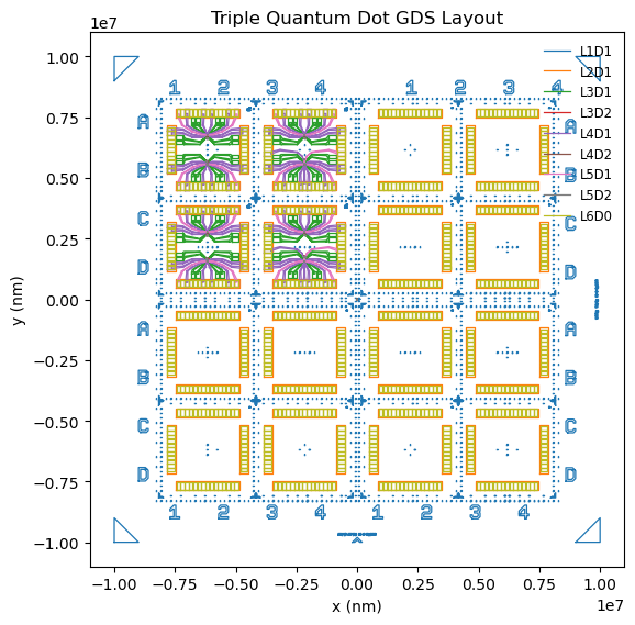
Before building the full 3D device, it is often useful to inspect the whole layout, locate the active region, and record the source-layer names you want to keep. The overview below uses polygon outlines rather than filled regions so it stays lighter on large GDS files.
from pathlib import Path

import matplotlib.pyplot as plt

from tempura.layout import crop_polygons_to_aoi, make_aoi_bbox_from_ranges, plot_layout_layers
from tempura.layout.readers import load_layout_data
layout_overview = plot_layout_layers(
    layout_data["polygons_by_layer"],
    title="Triple Quantum Dot GDS Layout",
    filled=False,
    coordinate_scale=nm_per_layout_unit,
    axis_unit="nm",
)
plt.show()
plt.close(layout_overview)
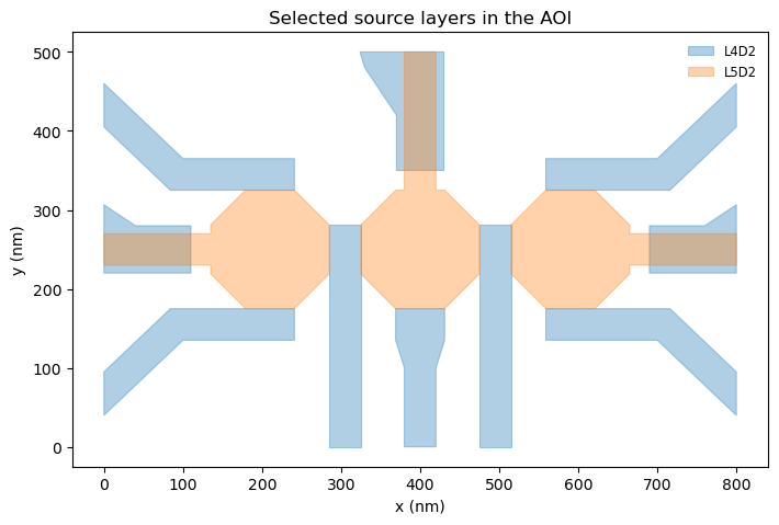
After locating the active region, record the source-layer names you want to carry into the device model and crop the AOI in the original layout coordinates.
selected_source_layers = ["L4D2", "L5D2"]
aoi_bbox = make_aoi_bbox_from_ranges(
    x_range=(-2170.4, -2169.6),
    y_range=(1569.75, 1570.25),
)
cropped = crop_polygons_to_aoi(layout_data["polygons_by_layer"], aoi_bbox)
figure = plot_layout_layers(
    cropped,
    layers=selected_source_layers,
    title="Selected source layers in the AOI",
    coordinate_scale=nm_per_layout_unit,
    axis_unit="nm",
)
plt.show()
plt.close(figure)
For the full end-to-end workflow, continue to Triple Quantum Dot.