Minimal Kitaev Chain
This page uses the minimal-Kitaev-chain layout as a second worked example of the public Tempura workflow:
- choose an area of interest from the source DXF file;
- rasterize that layout window with
prepare_layout(...); - describe the physical stack with an ordered
stack; - build the finalized
Devicewithbuild_device(...); - choose per-layer
resolution=[dx, dy, dz]values; - build and solve the
pescadoproblem; - inspect representative mesh cuts through the finalized problem.
For the generated reference API, see API Reference.
Core Ideas
The same contracts from the other layout-backed examples apply here:
prepare_layout(...)is the layout step;build_device(...)is the geometry step;- per-layer
resolution=[dx, dy, dz]is the meshing step; build_problem(...)assembles thepescadoelectrostatics problem;solve_gate_potentials(...)computes one basis response per gate;plot_problem_regions_with_mesh(...)visualizes cuts through the finalized mesh.
The important difference is that this example starts from a DXF file, so we use
size_mode="explicit_x" and supply the physical x length explicitly.
Worked Example
1. Define the source layout window
The first step is again geometric: select the part of the source layout that will become the simulation grid, choose the internal grid constant, and decide where the physical device window should be sampled.
from pathlib import Path

import matplotlib.pyplot as plt
import numpy as np

from tempura.electrostatics.pescado_wrapper import (
    build_problem,
    solve_gate_potentials,
)
from tempura.formatting import format_mapping_block, format_voltage
from tempura.layout.extraction import (
    make_aoi_bbox_from_ranges,
    plot_gate_stencil_layers,
    plot_layout_layers,
)
from tempura.layout.layout_pipeline import (
    build_device,
    format_device_dimensions,
    format_roi_summary,
    prepare_layout,
)
from tempura.plotting import (
    add_plane_cut_guides,
    make_xy_emphasis_axes,
    make_standard_plane_specs,
    nearest_axis_value,
    plot_problem_regions_with_mesh,
    plot_scalar_field_on_planes,
    transpose_plane_spec,
)

selected_layers = [
    "L18D0_Al_fine_A",
    "L1009D0_G1_fine_A",
    "L1014D0_G2_fine_A",
]
Units after prepare_layout(...)
This example also switches into Tempura's internal grid units after layout preparation.
If grid_constant_m = 20e-9, then one internal unit is 20 nm.
That means:
- the cropped AOI size is converted into grid units;
stackthicknesses are interpreted in those same grid units;- each layer's optional
resolution=[dx, dy, dz]is also written in those same grid units; - in
size_mode="explicit_x", the physicalxlength is fixed directly and theylength is inferred from the layout aspect ratio; - both physical ROI dimensions must be integer multiples of
grid_constant_m.
2. Define the physical stack and layer resolutions
The stack still describes the physical layer ordering from bottom to top.
Each gate entry names the source layout layer that should become one or more
Tempura Gate objects. The values below are already written directly in
Tempura's internal lattice units, so 1.0 means one grid_constant_m.
# The stack is written directly in internal units.
# With grid_constant_m = 20e-9, 1.0 means 20 nm.
# The top measurement gate is omitted here so the vertical cuts expose more of
# the buried gate stack in the later mesh plots.
stack = [
    {
        "kind": "dielectric",
        "name": "buffer",
        "permittivity": 12.9,
        "thickness": 4.0,
    },
    {
        "kind": "2deg",
        "name": "2deg",
        "permittivity": 12.9,
        "thickness": 1.0,
    },
    {
        "kind": "gate",
        "name": "gate_L18D0_Al_fine_A",
        "source_layer": "L18D0_Al_fine_A",
        "thickness": 1.0,
    },
    {
        "kind": "dielectric",
        "name": "blanket_1",
        "permittivity": 9.1,
        "thickness": 2.0,
    },
    {
        "kind": "gate",
        "name": "gate_L1009D0_G1_fine_A",
        "source_layer": "L1009D0_G1_fine_A",
        "thickness": 3.0,
    },
    {
        "kind": "dielectric",
        "name": "blanket_2",
        "permittivity": 9.1,
        "thickness": 2.0,
    },
    {
        "kind": "gate",
        "name": "gate_L1014D0_G2_fine_A",
        "source_layer": "L1014D0_G2_fine_A",
        "thickness": 4.0,
    },
]
3. Prepare the layout and apply the mask cleanup
prepare_layout(...) crops and rescales the DXF AOI in the same way as before,
but this example intentionally uses a smaller physical width than the older
1.5 um version so the resulting device region stays manageable at 20 nm.
It also needs two small layer-specific adjustments before we build the device:
- the ohmic layer is removed from the electrostatics gate stack;
- the aluminum opening is stored as an opening mask in the source layout, so we invert its rasterized stencil to obtain the metal region itself.
# Convert the chosen DXF window into Tempura's internal grid units.
prepared = prepare_layout(
    layout_path=examples_dir / "minimal_kitaev_chain.dxf",
    aoi_bbox=aoi_bbox,
    size_mode="explicit_x",
    grid_constant_m=grid_constant_m,
    physical_x_length=physical_x_length,
)

# Remove the ohmic source layer before building the electrostatic gate stack.
prepared["gate_stencils"].pop("L1005D0_ohmics_A", None)

# The aluminum opening is stored as an opening mask, so invert it to get metal.
if "L18D0_Al_fine_A" in prepared["gate_stencils"] and prepared["gate_stencils"]["L18D0_Al_fine_A"]:
    prepared["gate_stencils"]["L18D0_Al_fine_A"][0] = ~np.asarray(
        prepared["gate_stencils"]["L18D0_Al_fine_A"][0],
        dtype=bool,
    )

print(format_roi_summary(prepared))
ROI summary:
  layout_size: (1.0, 2.240000000000009)
  physical_size: (1e-06 m (1.0 um), 2.240000000000009e-06 m (2.240000000000009 um))
  grid_constant: 2e-08 m (0.02 um)
  rescaled_size: (50.0, 112.0)
  grid_shape: (ny=112, nx=50)
  grid_points: 5600
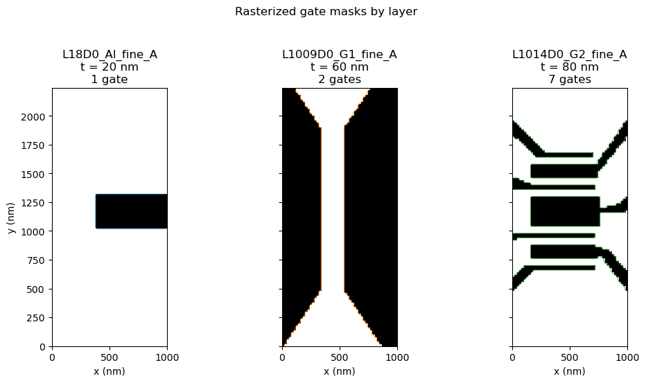
4. Inspect the layout layers used by the stack
At this stage we still have not built a Device. We are checking the selected
source layers and the rasterized masks that will become gates. Each panel below
shows one source layer with all disconnected gates from that layer overlaid.
figure = plot_gate_stencil_layers(
    prepared["gate_stencils"],
    roi_size=prepared["roi_size"],
    layer_order=selected_layers,
    title="Rasterized gate masks by layer",
    figsize=(10.8, 5.6),
    coordinate_scale=nm_per_unit,
    axis_unit="nm",
    layer_thicknesses={
        layer["source_layer"]: layer["thickness"]
        for layer in stack
        if layer["kind"] == "gate"
    },
)
plt.show()
plt.close("all")
5. Build the finalized Device
build_device(...) now consumes the prepared masks and produces a finalized
Tempura Device.
# build_device(...) consumes the masks and finalizes the 3D layer geometry.
device = build_device(prepared, stack)

print(format_device_dimensions(device, prepared))
Device summary:
  Lx: 50.0
  Ly: 112.0
  grid: 1.0
  grid_shape: (ny=112, nx=50)
  grid_points: 5600
  layers: buffer, 2deg, gate_L18D0_Al_fine_A_0, blanket_1, gate_L1009D0_G1_fine_A_0, gate_L1009D0_G1_fine_A_1, blanket_2, gate_L1014D0_G2_fine_A_0, gate_L1014D0_G2_fine_A_1, gate_L1014D0_G2_fine_A_2, gate_L1014D0_G2_fine_A_3, gate_L1014D0_G2_fine_A_4, gate_L1014D0_G2_fine_A_5, gate_L1014D0_G2_fine_A_6
  physical_size: (1e-06 m (1.0 um), 2.240000000000009e-06 m (2.240000000000009 um))
  grid_constant: 2e-08 m (0.02 um)
6. Mesh the device and solve the electrostatics problem
# Build the pescado problem directly from the finalized per-layer resolutions.
problem_builder, region_shapes, gate_names = build_problem(
    device,
    vacuum_scale=2.0,
    verbose=False,
)

# Solve one basis potential per gate and export the 2DEG bundle.
basis_potentials, problem = solve_gate_potentials(
    problem_builder,
    region_shapes,
    gate_names,
    rhs_block_size=1,
    verbose=False,
)
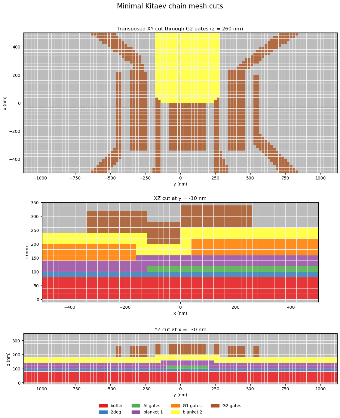
7. Inspect the finalized mesh
Before plotting, regroup the disconnected polygons back onto their source-layer
voltages and pin the displayed cuts to one central xz line and one yz line
at x = -20 nm.
def layer_voltage_for_gate(gate_name: str, layer_voltages: dict[str, float]) -> float:
    """Return the grouped source-layer voltage assigned to one solved gate."""
    for source_layer, voltage in layer_voltages.items():
        if gate_name.startswith(f"gate_{source_layer}"):
            return float(voltage)
    return 0.0
The figure below shows three stacked cuts through the finalized Pescado mesh:
one transposed xy plane through the patterned G2 layer at z = 260 nm,
one central xz cut, and one yz cut slightly left of center.
plot_region_shapes = dict(region_shapes)
plot_region_shapes.pop("Boundary", None)

region_display_names = {}
for region_name in region_shapes:
    if region_name.startswith("gate_L18D0_Al_fine_A"):
        region_display_names[region_name] = "Al gates"
    elif region_name.startswith("gate_L1009D0_G1_fine_A"):
        region_display_names[region_name] = "G1 gates"
    elif region_name.startswith("gate_L1014D0_G2_fine_A"):
        region_display_names[region_name] = "G2 gates"

coordinates = np.asarray(problem.coordinates, dtype=float)
x_cut = nearest_axis_value(coordinates, 0, -1.0)
y_cut = nearest_axis_value(coordinates, 1, 0.0)
mesh_xy_z = 13.0
mesh_plane_specs = make_standard_plane_specs(
    device,
    xy_title=f"XY cut through G2 gates (z = {mesh_xy_z * nm_per_unit:.0f} nm)",
    xy_plane_z=mesh_xy_z,
    xz_title=f"XZ cut at y = {y_cut * nm_per_unit:.0f} nm",
    xz_plane_y=y_cut,
    yz_title=f"YZ cut at x = {x_cut * nm_per_unit:.0f} nm",
    yz_plane_x=x_cut,
)
mesh_plane_specs["XY"] = transpose_plane_spec(
    mesh_plane_specs["XY"],
    title=f"Transposed XY cut through G2 gates (z = {mesh_xy_z * nm_per_unit:.0f} nm)",
)
plane_axes = [mesh_plane_specs["XY"], mesh_plane_specs["XZ"], mesh_plane_specs["YZ"]]
figure, axes = make_xy_emphasis_axes(
    figsize=(11.2, 13.8),
    layout="stack",
    height_ratios=(2.0, 1.1, 0.9),
)

figure, _ = plot_problem_regions_with_mesh(
    problem,
    plot_region_shapes,
    plane_axes,
    axes=axes,
    region_display_names=region_display_names,
    suptitle="Minimal Kitaev chain mesh cuts",
    show_volume_edges=True,
    show_mesh_points=False,
    tile_edgecolors="#f3f3f3",
    coordinate_scale=nm_per_unit,
    axis_unit="nm",
)
add_plane_cut_guides(axes[0], x=y_cut, y=x_cut, coordinate_scale=nm_per_unit)
plt.show()
plt.close(figure)
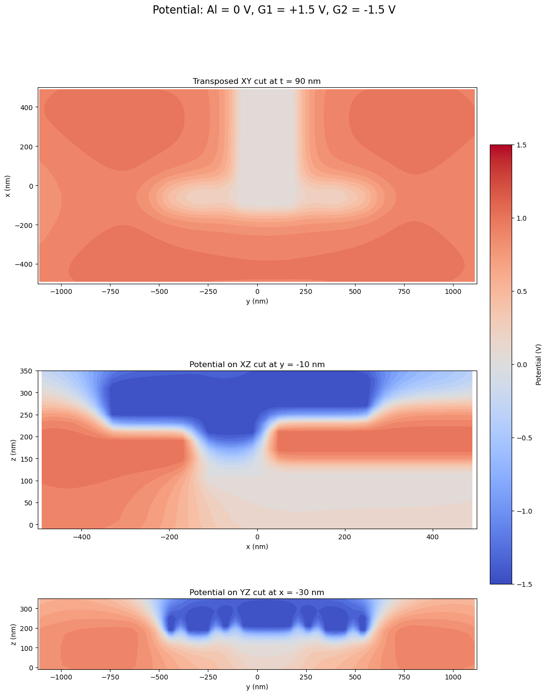
8. Show A Dot-Like Voltage Configuration On The 2DEG Plane
The solved basis is still per disconnected polygon, but a static voltage state
is easier to read when grouped back by source layer. The combination below
highlights two dot-like islands along the G2-defined chain, and potential_vmin
and potential_vmax expose the displayed color scale directly.
layer_voltages = {
    "L18D0_Al_fine_A": 0.,
    "L1009D0_G1_fine_A": 1,
    "L1014D0_G2_fine_A": -1.5,
}
potential_vmin = -1.5
potential_vmax = 1.5
combined_field = np.zeros(problem.coordinates.shape[0], dtype=float)
for gate_name in gate_names:
    combined_field += layer_voltage_for_gate(gate_name, layer_voltages) * basis_potentials[gate_name]
potential_xy_z = nearest_axis_value(
    coordinates,
    2,
    float(np.asarray(device.layers["2deg"].shape.bbox, dtype=float)[1, 2]),
)
potential_plane_specs = make_standard_plane_specs(
    device,
    xy_title=f"Potential on XY cut at t = {potential_xy_z * nm_per_unit:.0f} nm",
    xy_plane_z=potential_xy_z,
    xz_title=f"Potential on XZ cut at y = {y_cut * nm_per_unit:.0f} nm",
    xz_plane_y=y_cut,
    yz_title=f"Potential on YZ cut at x = {x_cut * nm_per_unit:.0f} nm",
    yz_plane_x=x_cut,
)
potential_plane_specs["XY"] = transpose_plane_spec(
    potential_plane_specs["XY"],
    title=f"Transposed XY cut at t = {potential_xy_z * nm_per_unit:.0f} nm",
)

fig, axes = make_xy_emphasis_axes(
    figsize=(11.2, 14.6),
    layout="stack",
    height_ratios=(2.0, 1.1, 0.9),
)
fig, axes = plot_scalar_field_on_planes(
    problem,
    combined_field,
    [
        potential_plane_specs["XY"],
        potential_plane_specs["XZ"],
        potential_plane_specs["YZ"],
    ],
    axes=axes,
    suptitle="Potential: Al = 0 V, G1 = +1.5 V, G2 = -1.5 V",
    colorbar_label="Potential (V)",
    vmin=potential_vmin,
    vmax=potential_vmax,
    symmetric=potential_vmin is None and potential_vmax is None,
    coordinate_scale=nm_per_unit,
    axis_unit="nm",
)
print(format_mapping_block("Layer voltages", layer_voltages, value_formatter=format_voltage))
plt.show()
plt.close(fig)
Layer voltages:
  L18D0_Al_fine_A: +0.00 V
  L1009D0_G1_fine_A: +1.00 V
  L1014D0_G2_fine_A: -1.50 V